5.4.3. Storage Circuits
Storage circuits are used to construct computer memory for storing binary values. The type of computer memory built from storage circuits is called static RAM (SRAM). It is used to build CPU register storage and on-chip cache memory. Systems typically use dynamic RAM (DRAM) for main memory (RAM) storage. The capacitor-based design of DRAM requires that it be periodically refreshed with the value it stores, hence the "dynamic" moniker. SRAM is circuit-based storage that does not need to have its values refreshed, thus it is referred to as static RAM. Circuit-based memory is faster but more expensive than capacitor-based memory. As a result, SRAM tends to be used for storage at the top of the memory hierarchy (CPU registers and on-chip cache memory), and DRAM for main memory (RAM) storage. In this chapter, we focus on circuit-based memory like SRAM.
To store a value, a circuit must contain a feedback loop so that the value is retained by the circuit. In other words, a storage circuit’s value depends on its input values and also its currently stored value. When the circuit stores a value, its currently stored value and its inputs together produce an output that matches the currently stored value (i.e. the circuit continues to store the same value). When a new value is written into a storage circuit, the circuit’s input values change momentarily to modify the behavior of the circuit, which results in a new value being written into and stored in the circuit. Once written, the circuit resumes a steady state of storing the newly written value until the next write to the circuit occurs.
RS Latch
A latch is a digital circuit that stores (or remembers) a 1-bit value. One example is a reset-set latch (or RS latch). An RS latch has two input values, S and R, and one output value, Q, which is also the value stored in the latch. An RS latch may additionally output NOT(Q), the negation of the stored value. Figure 1 shows an RS latch circuit for storing a single bit.
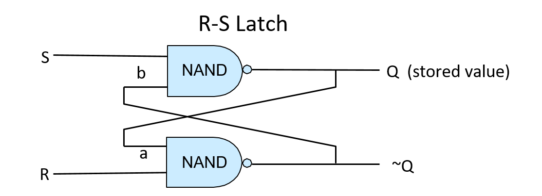
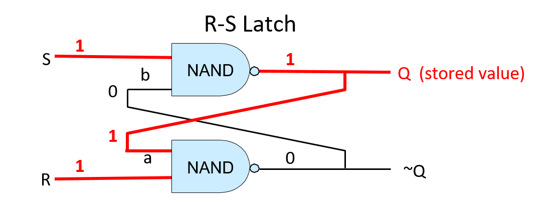
The first thing to note about the RS latch is the feedback loop from its outputs to its inputs: the output of the top NAND gate (Q) is input (a) to the bottom NAND gate, and the output of the bottom NAND gate (~Q) is input (b) to the top NAND gate. When inputs S and R are both 1, the RS latch stores the value Q. In other words, when S and R are both 1, the RS latch output value Q is stable. To see this behavior, consider Figure 2; this shows an RS latch that stores the value 1 (Q is 1). When R and S are both 1, the feedback input value (a) to the bottom NAND gate is the value of Q, which is 1, so the output of the bottom NAND gate is 0 (1 NAND 1 is 0). The feedback input value (b) to the top NAND gate is the output of the bottom NAND gate, which is 0. The other input to the top NAND gate is 1, the value of S. The output of the top gate is 1 (1 NAND 0 is 1). Thus, when S and R are both 1, this circuit continuously stores the value of Q (1 in this example).
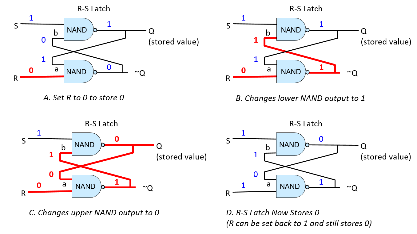
To change the value stored in an RS latch, the value of exactly one of R or S is set to 0. When the latch stores the new value, R and S are set back to 1. Control circuitry around the RS latch ensures that R and S can never simultaneously be 0: at most one of them will have a value 0, and a value of 0 for one of R or S means that a value is being written into the RS latch. To store the value 0 in an RS latch, input R is set to 0 (and the value of S stays at 1). To store the value 1 in an RS latch, input S is set to 0 (and the value of R stays at 1). For example, assume that the RS latch currently stores 1. To write 0 into the latch, R’s value is set to 0. This means that the values 0 and 1 are input to the lower NAND gate which computes the result of (0 NAND 1), or is 1. This output value of 1 is also input b to the top NAND gate (shown in Figure 3 B). With a new b input value of 1 and the S input value 1, the upper NAND gate computes a new output value 0 for Q, which is also fed as input a into the lower NAND gate (shown in Figure 3 C). With a’s value 0 and b’s value 1, the latch now stores 0. When R is eventually set back to 1 the RS latch continues to store the value 0 (shown in Figure 3 D).
Gated D Latch
A gated D latch adds circuitry to an RS latch to ensure that it never receives an input of 0 to both R and S simultaneously. Figure 4 shows the construction of a gated D latch.
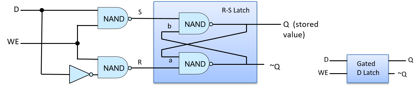
The data input (D) to the gated D latch is the value to store into the circuit (either 0 or 1). The Write Enable (WE) input controls writing a value into the RS latch. When WE is 0, the output from both NAND gates is 1, resulting in S and R input values of 1 to the RS latch (the RS latch stores a value). The gated D latch writes the value of D into the RS latch only when WE is 1. Because the data input (D) value is inverted before it is sent to the bottom NAND gate, the input of only one of the top or bottom NAND gates input is 1. This means that when the WE bit is 1, exactly one of R or S is 0. For example, when D is 1 and WE is 1, the top NAND computes (1 NAND 1) and the bottom NAND gate computes (O NAND 1). As a result, the input to S from the top NAND gate is 0 and the input to R from the bottom NAND gate is 1, resulting in writing the value 1 into the RS latch. When the WE input is 0, both NAND gates output 1, keeping R and S at 1. In other words, when WE is 0, the value of D has no effect on the value stored in the RS latch; only when WE is 1 is the value of D written into the latch. To write another value into the gated D latch, set D to the value to store and WE to 1.
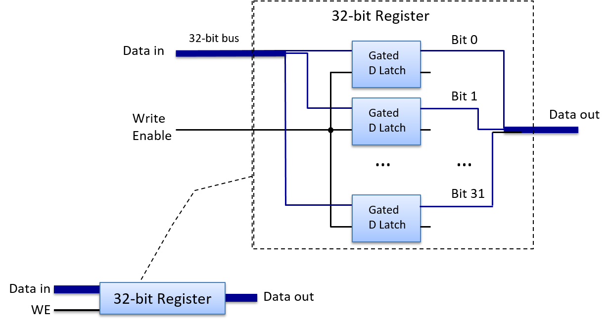
CPU Register
Multibit storage circuits are built by linking several 1-bit storage circuits together. For example, combining 32 1-bit D latches together yields a 32-bit storage circuit that could be used as a 32-bit CPU register, as shown in Figure 5. The register circuit has two input values: a 32-bit data value and a 1-bit Write Enable signal. Internally, each 1-bit D latch takes as its D input one bit of the register’s 32-bit Data in input, and each 1-bit D latch takes the register’s WE input as its WE input. The register’s output is the 32-bit value stored across the 32 1-bit D latches that make up the register circuit.