5.5. Building a Processor: Putting It All Together
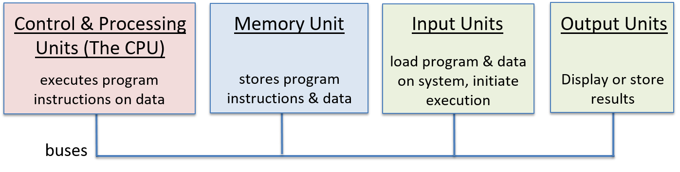
The central processing unit (CPU) implements the processing and control units of the von Neumann architecture, the parts that drive the execution of program instructions on program data (see Figure 1).
The CPU is constructed from basic arithmetic/logic, storage, and control circuit building blocks. Its main functional components are the arithmetic logic unit (ALU), which performs arithmetic and logic operations; a set of general-purpose registers for storing program data; some control circuitry and special-purpose registers that are used in the implementation of instruction execution; and a clock that drives the circuitry of the CPU to execute program instructions.
In this section, we present the main parts of the CPU, including the ALU and register file, and show how they are combined to implement a CPU. In the next section, we discuss how the CPU executes program instructions and how the clock is used to drive the execution of program instructions.
5.5.1. The ALU
The ALU is a complex circuit that implements all arithmetic and logic operations on signed and unsigned integers. A separate floating-point unit performs arithmetic operations on floating-point values. The ALU takes integer operand values and an opcode value that specifies the operation to perform (e.g. addition). The ALU outputs the resulting value of performing the specified operation on the operand inputs and condition code values that encode information about the result of the operation. Common condition codes specify whether the ALU result is negative, zero, or if there is a carry-out bit from the operation. For example, given the C statement
x = 6 + 8;the CPU begins executing the addition by feeding the operand values (6 and 8) and the bits that encode an ADD operation to the ALU circuit. The ALU computes the result and outputs it along with condition codes to indicate that the result is nonnegative, is nonzero, and causes no carry-out. Each condition code is encoded in a single bit. A bit value of 1 indicates that the condition holds, and a bit value of 0 indicates that it does not hold for the ALU result. In our example, the bit pattern 000 specifies the set of three conditions associated with executing 6+8: the result is not negative (0), is not zero (0), and the carry-out value is zero (0).
Condition codes, set by the ALU as part of its execution of an operation,
are sometimes used by subsequent instructions that choose an action
based on a particular condition. For example, an ADD instruction
can compute the (x + 8) part of the following if statement:
if( (x + 8) != 0 ) {
    x++;
}
The ALU’s execution of the ADD instruction sets condition codes based on
the result of adding (x + 8). A conditional jump instruction executed
after the ADD instruction tests the condition code bits set by
the ADD instruction and either jumps
(skips over executing the instructions in the if body) or not
based on their value.
For example, if the ADD instruction sets the zero condition code to 0,
the conditional jump instruction will not jump past the instructions
associated with the if body (0 for the zero condition code means that the
result of the ADD was not zero). If the zero condition code is 1, it will
jump past the if body instructions.
To implement a jump past a set of instructions, the CPU writes
the memory address of the first instruction after the if body
instructions into the program counter (PC), which contains the address
of the next instruction to execute.
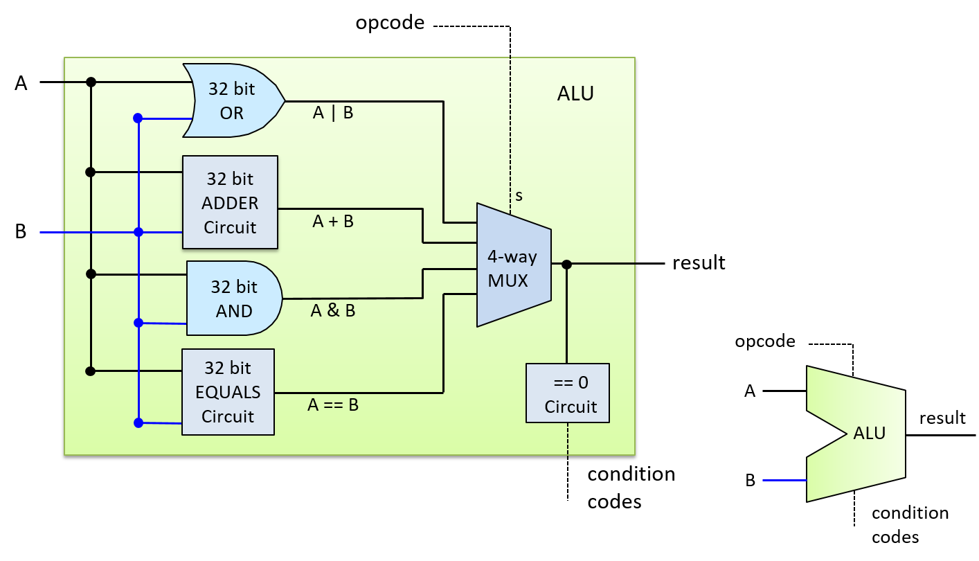
An ALU circuit combines several arithmetic and logic circuits (for implementing its set of operations) with a multiplexer circuit to pick the ALU’s output. Rather than trying to selectively activate only the arithmetic circuit associated with the specific operation, a simple ALU sends its operand input values to all of its internal arithmetic and logic circuits. The output from all of the ALU’s internal arithmetic and logic circuits are input to its multiplexer circuit, which chooses the ALU’s output. The opcode input to the ALU is used as the signal input to the multiplexer to select which arithmetic/logic operation to select as the ALU’s output. Condition code output is based on the MUX output combined with circuitry to test the output’s value to determine each condition code bit.
Figure 2 shows an example ALU circuit that performs four different operations (ADD, OR, AND, and EQUALS) on two 32-bit operands. It also produces a single condition code output that indicates whether the result of the operation is zero. Notice that the ALU directs the opcode to a multiplexer that selects which of the ALU’s four arithmetic results it outputs.
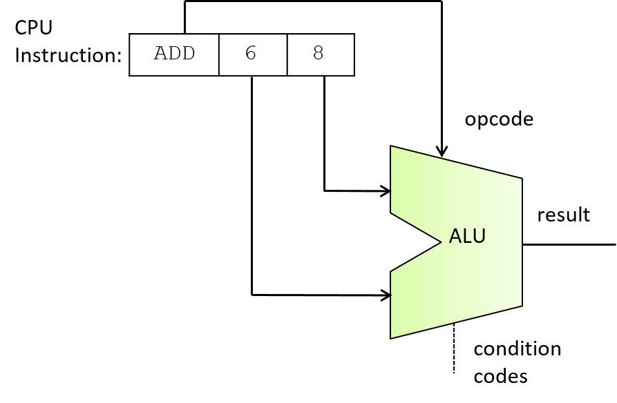
The opcode input to the ALU comes from bits in the instruction that the CPU is executing. For example, the binary encoding for an ADD instruction might consist of four parts:
| OPCODE BITS | OPERAND A SOURCE | OPERAND B SOURCE | RESULT DESTINATION |
Depending on the CPU architecture, operand source bits might encode a CPU register, the memory address storing the operand value, or literal operand values. For example, in an instruction to perform 6 + 8, the literal values 6 and 8 could be encoded directly into the operand specifier bits of the instruction.
For our ALU, the opcode requires two bits because the ALU supports four operations, and two bits can encode four distinct values (00, 01, 10, 11), one for each operation. In general, an ALU that performs N distinct operations, needs log2(N) opcode bits to specify which operation result to output from the ALU.
Figure 3 shows an example of how the opcode and operand bits of an ADD instruction are used as input into our ALU.
5.5.2. The Register File
At the top of the memory hierarchy, the CPU’s set of general-purpose registers store temporary values. CPUs provide a very small number of registers, commonly 8-32 (e.g., the IA32 architecture provides 8, MIPS provides 16, and ARM provides 13). Instructions often get their operand values from, or store their results to, general-purpose registers. For example, an ADD instruction may be encoded as "add the value from Register 1 to the value from Register 2 and store the result in Register 3".
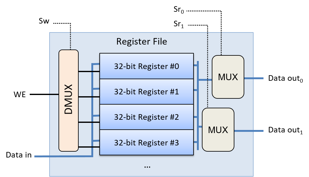
The CPU’s set of general-purpose registers is organized into a register file circuit. A register file consists of a set of register circuits for storing data values and some control circuits for controlling reads and writes to its registers. The circuit typically has a single data input line for the value to write into one of its registers, and two data output lines for simultaneously reading two values from its registers.
Figure 4 shows an example of a register file circuit with four registers. Its two output values (Data out0 and Data out1) are controlled by two multiplexer circuits. Each of its read selection inputs (Sr0 and Sr1) is fed into one of the MUXs to pick the register value for the corresponding output. The data input to the register file (the Data in line) is sent to every register circuit, and its write enable (WE) input is fed through a demultiplexer (DMUX) circuit first before being sent to each register circuit. A DMUX circuit takes one input value and chooses which of N outputs to send the value to, sending the remaining N-1 outputs 0. The write selection input (Sw) to the register file is sent to the DMUX circuit to choose the WE value’s destination register. When the register file’s WE input value is 0, no value is written into a register because each register’s WE bit also gets 0 (thus, Data in has no effect on the values stored in the registers). When the WE bit is 1, the DMUX outputs a WE bit value of 1 to only the register specified by the write selection input (Sw), resulting in the Data in value being written to the selected register only.
Special-Purpose Registers
In addition to the set of general-purpose registers in the register file, a CPU contains special-purpose registers that store the address and content of instructions. The program counter (PC) stores the memory address of the next instruction to execute, and the instruction register (IR) stores the bits of the current instruction being executed by the CPU. The bits of the instruction stored in the IR are used as input into different parts of the CPU during the instruction’s execution. We discuss these registers in more detail in the next section on instruction execution.
5.5.3. The CPU
With the ALU and register file circuits, we can build the main parts of the CPU, as shown in Figure 5. Because instruction operands often come from values stored in general-purpose registers, the register file’s outputs send data to the ALU’s inputs. Similarly, because instruction results are often stored in registers, the ALU’s result output is sent as input to the register file. The CPU has additional circuitry to move data between the ALU, register file, and other components (e.g., main memory).
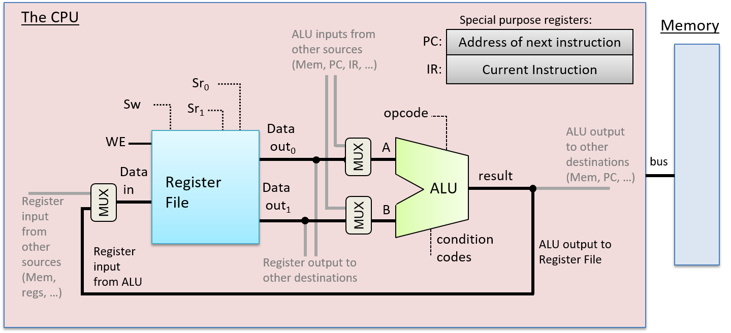
These main parts of the CPU make up its data path. The data path consists of the parts of the CPU that perform arithmetic and logic operations (the ALU) and store data (registers), and the buses that connect these parts. The CPU also implements a control path that drives the execution of program instructions by the ALU on operands stored in the register file. Additionally, the control path issues commands to I/O devices and coordinates memory accesses as needed by instructions. For example, some instructions may get their operand values directly from (or store their results directly to) memory locations rather than general-purpose registers. In the next section, we focus our discussion of CPU instruction execution on instructions that get operand values and store results to the register file. The CPU requires additional control circuitry to read operand values or to write instruction results to other locations, but the main instruction execution steps behave the same regardless of the source and destination locations.