5.4.1. Arithmetic and Logic Circuits
Arithmetic and Logic circuits implement the arithmetic and logic instructions of an ISA that together make up the arithmetic logic unit (ALU) of the processor. Arithmetic and logic circuits also implement parts of other functionality in the CPU. For example, arithmetic circuits are used to increment the program counter (PC) as part of the first step of instruction execution, and they are used to calculate memory addresses by combining instruction operand bits and register values.
Circuit design often starts with implementing a 1-bit version of a simple circuit from logic gates. This 1-bit circuit is then used as a building block for implementing M-bit versions of the circuit. The steps for designing a 1-bit circuit from basic logic gates are:
-
Design the truth table for the circuit: determine the number of inputs and outputs, and add a table entry for every permutation of input bit(s) that specifies the value of the output bit(s).
-
Using the truth table, write an expression for when each circuit output is 1 in terms of its input values combined with AND, OR, NOT.
-
Translate the expression into a sequence of logic gates, where each gate gets its inputs from either an input to the circuit or from the output of a preceding logic gate.
We follow these steps to implement a single-bit equals
circuit: bitwise equals (A == B) outputs 1 when the values of A and B are
the same, and it outputs 0 otherwise.
First, design the truth table for the circuit:
| A | B | A == B output |
|---|---|---|
0 |
0 |
1 |
0 |
1 |
0 |
1 |
0 |
0 |
1 |
1 |
1 |
Next, write expressions for when A == B is 1 in terms of A and B combined
with AND, OR, and NOT. First, consider each row whose output
is 1 separately, starting with the first row in the truth table:
| A | B | A == B |
|---|---|---|
0 |
0 |
1 |
For the input values in this row, construct a conjunction of expressions of its inputs that evaluate to 1. A conjunction combines subexpressions that evaluate to 0 or 1 with AND, and is itself 1 only when both of its subexpressions evaluate to 1. Start by expressing when each input evaluates to 1:
NOT(A)    # is 1 when A is 0
NOT(B)    # is 1 when B is 0
Then, create their conjunction (combine them with AND) to yield an expression for when this row of the truth table evaluates to 1:
NOT(A) AND NOT(B) # is 1 when A and B are both 0
We do the same thing for the last row in the truth table, whose output is also 1:
| A | B | A == B |
|---|---|---|
1 |
1 |
1 |
A AND B # is 1 when A and B are both 1
Finally, create a disjunction (an OR) of each conjunction corresponding to a row in the truth table that evaluates to 1:
(NOT(A) AND NOT(B)) OR (A AND B) # is 1 when A and B are both 0 or both 1
At this point we have an expression for A == B that can be translated to a
circuit. At this step, circuit designers employ techniques
to simplify the expression to create a minimal equivalent expression (one
that corresponds to the fewest operators and/or shortest path length of
gates through the circuit). Designers must take great care when minimizing
a circuit design to ensure the equivalence of the translated expression.
There are formal methods for circuit minimization that
are beyond the scope of our coverage, but we will employ a few heuristics
as we develop circuits.
For our example, we directly translate the preceding expression to a circuit. We may be tempted to replace (NOT(A) AND NOT(B)) with (A NAND B), but note that these two expressions are not equivalent: they do not evaluate the same for all permutations of A and B. For example, when A is 1 and B is 0, (A == B) is 0 and (A NAND B) is 1.
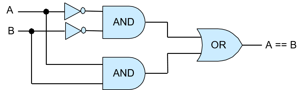
To translate the expression to a circuit, start from the innermost expression and work outward (the innermost will be the first gates, whose outputs will be inputs to subsequent gates). The first set of gates correspond to any negation of input values (NOT gates of inputs A and B). Next, for each conjunction, create parts of the circuit feeding input values into an AND gate. The AND gate outputs are then fed into OR gate(s) representing the disjunction. The resulting circuit is shown in Figure 1.
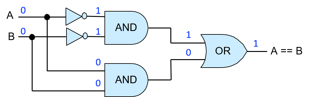
To verify the correctness of this circuit, simulate all possible permutations of input values A and B through the circuit and verify that the output of the circuit matches its corresponding row in the truth table for (A == B). For example, if A is 0 and B is 0, the two NOT gates negate their values before being fed through the top AND gate, so the input to this AND gate is (1, 1), resulting in an output of 1, which is the top input value to the OR gate. The values of A and B (0, 0) are fed directly though the bottom AND gate, resulting in output of 0 from the bottom AND gate, which is the lower input to the OR gate. The OR gate thus receives input values (1, 0) and outputs the value 1. So, when A and B are both 0, the circuit correctly outputs 1. Figure 2 illustrates this example.
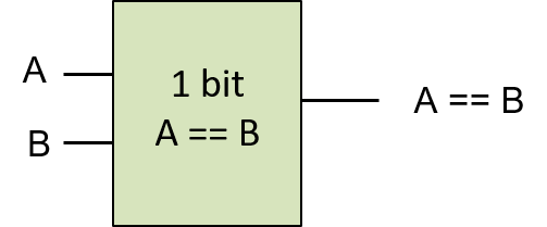
Viewing the implementation of a 1-bit equality circuit as a unit allows it to be abstracted from its implementation, and thus it can be more easily used as a building block for other circuits. We represent this abstraction of the 1-bit equality circuit (shown in Figure 3) as a box with its two inputs labeled A and B and its single output labeled A == B. The internal gates that implement the 1-bit equality circuit are hidden in this abstracted view of the circuit.
Single-bit versions of NAND, NOR, and XOR circuits can be constructed similarly, using only AND, OR, and NOT gates, starting with their truth tables (Table 2) and applying the same steps as the 1-bit equality circuit.
| A | B | A NAND B | A NOR B | A XOR B |
|---|---|---|---|---|
0 |
0 |
1 |
1 |
0 |
0 |
1 |
1 |
0 |
1 |
1 |
0 |
1 |
0 |
1 |
1 |
1 |
0 |
0 |
0 |
Multibit versions of these circuits are constructed from multiple single-bit versions of the circuits in a similar way to how the 4-bit AND gate was constructed from four 1-bit AND gates.
Arithmetic Circuits
Arithmetic circuits are constructed using exactly the same method as we used for constructing the logic circuits. For example, to construct a 1-bit adder circuit, start with the truth table for single-bit addition, which has two input values, A and B, and two output values, one for the SUM of A and B, and another output for overflow or CARRY OUT. Table 3 shows the resulting truth table for 1-bit add.
| A | B | SUM | CARRY OUT |
|---|---|---|---|
0 |
0 |
0 |
0 |
0 |
1 |
1 |
0 |
1 |
0 |
1 |
0 |
1 |
1 |
0 |
1 |
In the next step, for each output, SUM and CARRY OUT, create logical expressions of when the output value is 1. These expressions are expressed as disjunctions of per-row conjunctions of input values:
SUM: (NOT(A) AND B) OR (A AND NOT(B))     # 1 when exactly one of A or B is 1
CARRY OUT:  A AND B                       # 1 when both A and B are 1
The expression for CARRY OUT cannot be simplified. However, the expression for SUM is more complicated and can be simplified, leading to a simpler circuit design. The first thing to note is that the SUM output can also be expressed as (A XOR B). If we have an XOR gate or circuit, expressing SUM as (A XOR B) results in a simpler adder circuit design. If not, the expression using AND, OR, and NOT is used and implemented using AND, OR, and NOT gates.
Let’s assume that we have an XOR gate that we can use for implementing the 1-bit adder circuit. The resulting circuit is shown in Figure 4.
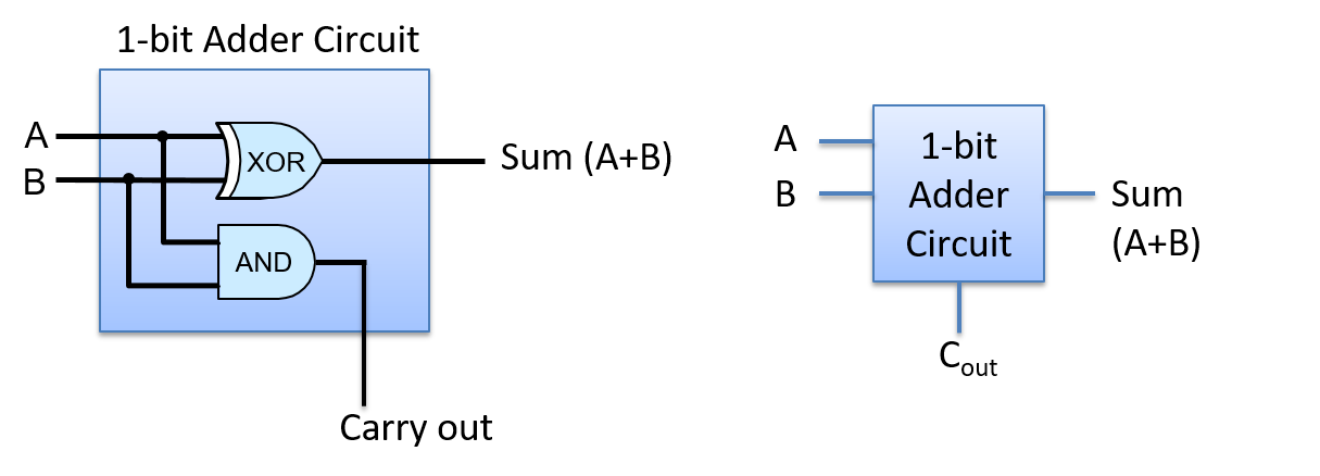
The 1-bit adder circuit can be used as a building block for more complicated circuits. For example, we may want to create N-bit adder circuits for performing addition on values of different sizes (e.g. 1-byte, 2-byte, or 4-byte adder circuits). However, creating an N-bit adder circuit from N 1-bit adder circuits requires more care than creating an N-bit logic circuits from N 1-bit logic circuits.
When performing a multibit addition (or subtraction), individual bits are summed in order from the least significant bit to the most significant bit. As this bitwise addition proceeds, if the sum of the ith bits results in a carry out value of 1, then an additional 1 is added with the two (i+1)st bits. In other words, the carry out of the ith bit adder circuit is an input value to the (i+1)st bit adder circuit.
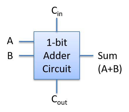
Thus, to implement a multibit adder circuit, we need a new 1-bit adder circuit that has three inputs: A, B, and CARRY IN. To do this, follow the steps above for creating a 1-bit adder circuit, with three inputs (A, B, CARRY IN) and two outputs (SUM and CARRY OUT), starting with the truth table for all possible permutations of its three inputs. We leave the design of this circuit as an exercise for the reader, but we show its abstraction as a 1-bit adder circuit in Figure 5.
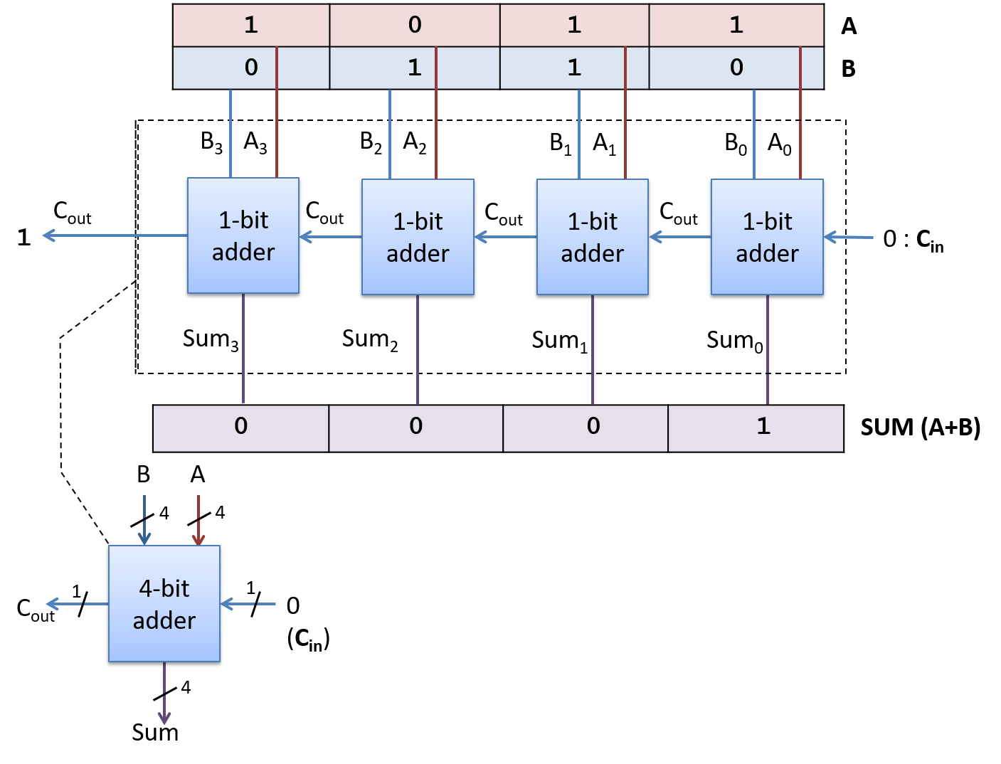
Using this version of a 1-bit adder circuit as a building block, we can construct an N-bit adder circuit by feeding corresponding operand bits through individual 1-bit adder circuits, feeding the CARRY OUT value from the ith 1-bit adder circuit into the CARRY IN value of the (i+1)st 1-bit adder circuit. The 1-bit adder circuit for the 0th bits receives a value of 0 for its CARRY IN from another part of the CPU circuitry that decodes the ADD instruction.
This type of N-bit adder circuit, built from N 1-bit adder circuits, is called a ripple carry adder, shown in Figure 6. The SUM result ripples or propagates through the circuit from the low-order to the high-order bits. Only after bit 0 of the SUM and CARRY OUT values are computed will the bit 1 of the SUM and CARRY OUT be correctly computed. This is because the 1st bit’s CARRY IN gets its value from the 0th bit’s CARRY OUT, and so on for subsequent higher-order bits of the result.
Circuits for other arithmetic and logic functions are constructed in similar ways by combining circuits and logic gates. For example, a subtraction circuit that computes (A - B) can be built from adder and negation circuits that compute subtraction as (A + (-B)).