5.6. The Processor’s Execution of Program Instructions
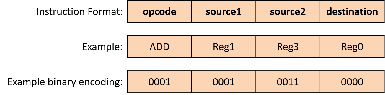
Instruction execution is performed in several stages. Different architectures implement different numbers of stages, but most implement the Fetch, Decode, Execute, and WriteBack phases of instruction execution in four or more discrete stages. In discussing instruction execution, we focus on these four stages of execution, and we use an ADD instruction as our example. Our ADD instruction example is encoded as shown in Figure 1.
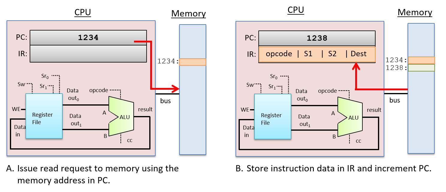
To execute an instruction, the CPU first fetches the
next instruction from memory into a special-purpose register, the
instruction register (IR). The memory address of the instruction to fetch
is stored in another special-purpose register, the program counter (PC).
The PC keeps track of the memory address of the
next instruction to fetch and is incremented
as part of executing the fetch stage, so that it stores the value
of the very next instruction’s memory address. For example, if all
instructions are 32 bits long, then the PC’s value is incremented by 4
(each byte, 8 bits, has a unique address) to store the memory address of
the instruction immediately following the one being fetched. Arithmetic
circuits that are separate from the ALU increment the PC’s value.
The PC’s value may also change during the WriteBack stage.
For example, some instructions jump to specific addresses, such as those
associated with the execution of loops, if-else, or function calls.
Figure 2 shows the fetch stage of execution.
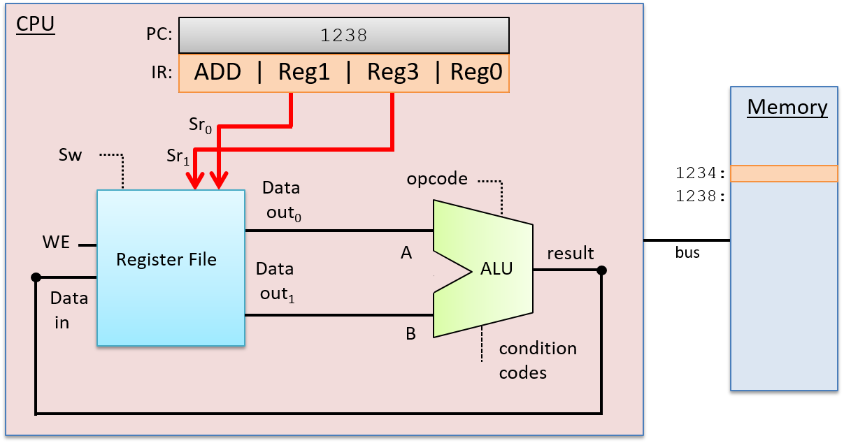
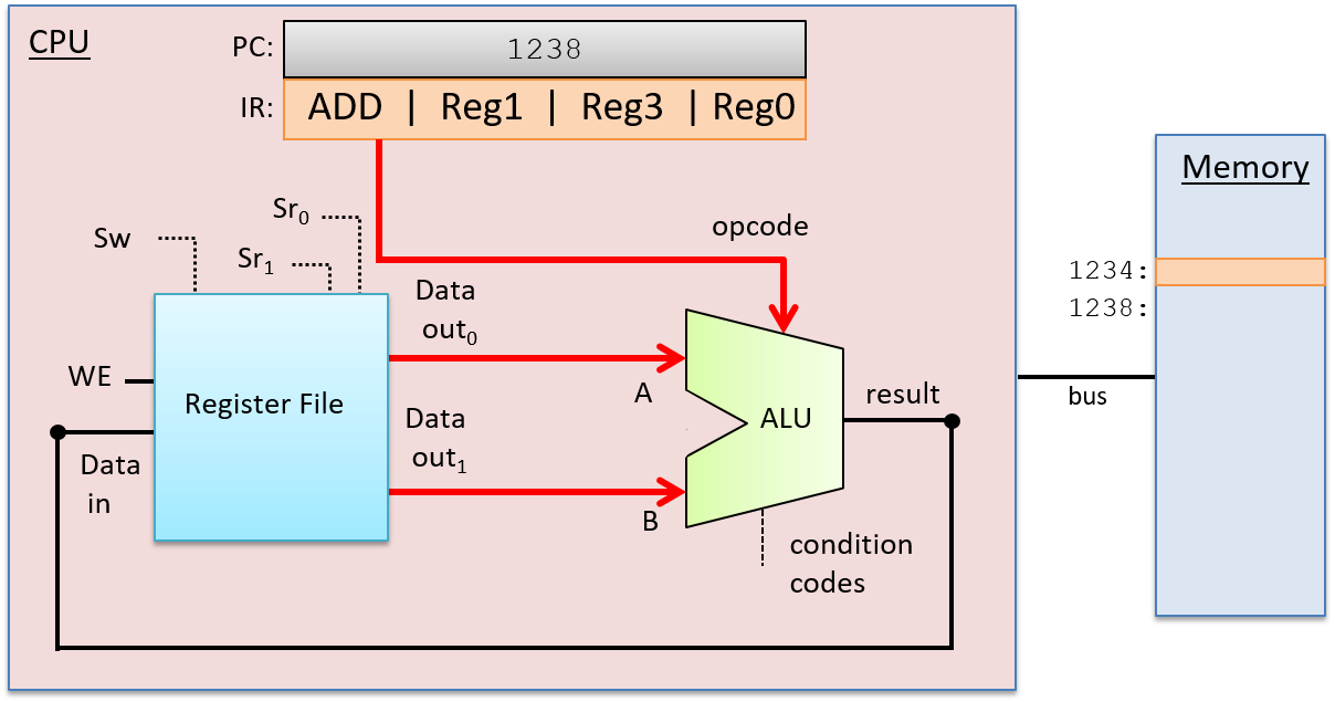
After fetching the instruction, the CPU decodes the instruction bits stored in the IR register into four parts: the high-order bits of an instruction encode the opcode, which specifies the operation to perform (e.g. ADD, SUB, OR, …), and the remaining bits are divided into three subsets that specify the two operand sources and the result destination. In our example, we use registers for both sources and the result destination. The opcode is sent on wires that are input to the ALU and the source bits are sent on wires that are inputs to the register file. The source bits are sent to the two read selection inputs (Sr0 and Sr1) that specify which register values are read from the register file. The Decode stage is shown in Figure 3.
After the Decode stage determines the operation to perform and the operand sources, the ALU performs the operation in the next stage, the Execution stage. The ALU’s data inputs come from the two outputs of the register file, and its selection input comes from the opcode bits of the instruction. These inputs propagate through the ALU to produce a result that combines the operand values with the operation. In our example, the ALU outputs the result of adding the value stored in Reg1 to the value stored in Reg3, and outputs the condition code values associated with the result value. The Execution stage is shown in Figure 4.
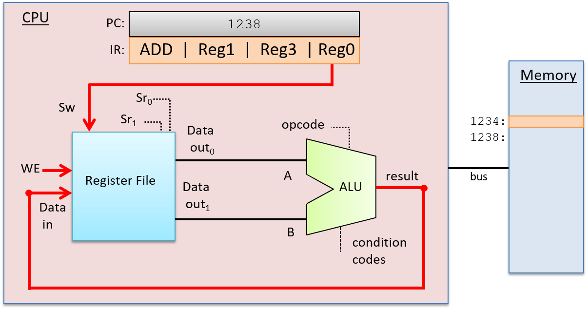
In the WriteBack stage, the ALU result is stored in the destination register. The register file receives the ALU’s result output on its Data in input, the destination register (from instructions bits in the IR) on its write-select (Sw) input, and 1 on its WE input. For example, if the destination register is Reg0, then the bits encoding Reg0 in the IR are sent as the Sw input to the register file to pick the destination register. The output from the ALU is sent as the Data in input to the register file, and the WE bit is set to 1 to enable writing the ALU result into Reg0. The WriteBack stage is shown in Figure 5.
5.6.1. Clock-Driven Execution
A clock drives the CPU’s execution of instructions, triggering the start of each stage. In other words, the clock is used by the CPU to determine when inputs to circuits associated with each stage are ready to be used by the circuit, and it controls when outputs from circuits represent valid results from one stage and can be used as inputs to other circuits executing the next stage.
A CPU clock measures discrete time as opposed to continuous time. In other
words, there exists a time 0, followed by a time 1, followed by a time 2, and
so on for each subsequent clock tick. A processor’s clock cycle time
measures the time between each clock tick. A processor’s clock speed (or
clock rate) is 1/(clock cycle time). It is typically measured in megahertz
(MHz) or gigahertz (GHz). A 1-MHz clock rate has one million clock ticks per
second, and 1-GHz has one billion clock ticks per second. The clock rate is a
measure of how fast the CPU can run, and is an estimate of the maximum number
of instructions per second a CPU can execute. For example, on simple scalar
processors like our example CPU, a 2-GHz processor might achieve a maximum
instruction execution rate of two billion instructions per second (or two
instructions every nanosecond).
Although increasing the clock rate on a single machine will improve its performance, clock rate alone is not a meaningful metric for comparing the performance of different processors. For example, some architectures (such as RISC) require fewer stages to execute instructions than others (such as CISC). In architectures with fewer execution stages a slower clock may yield the same number of instructions completed per second as on another architecture with a faster clock rate but more execution stages. For a specific microprocessor, however, doubling its clock speed will roughly double its instruction execution speed.
The Clock Circuit
A clock circuit uses an oscillator circuit to generate a very precise and regular pulse pattern. Typically, a crystal oscillator generates the base frequency of the oscillator circuit, and the pulse pattern of the oscillator is used by the clock circuit to output a pattern of alternating high and low voltages corresponding to an alternating pattern of 1 and 0 binary values. Figure 6 shows an example clock circuit generating a regular output pattern of 1 and 0.
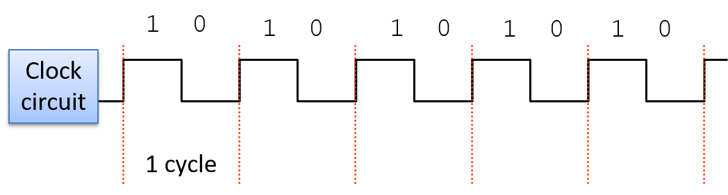
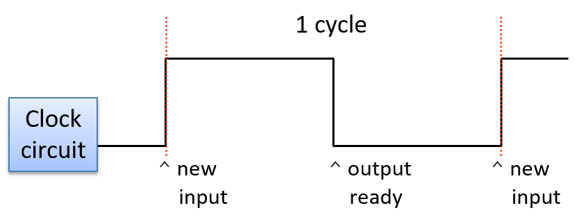
A clock cycle (or tick) is a 1 and 0 subsequence from the clock circuit pattern. The transition from a 1 to a 0 or a 0 to a 1 is called a clock edge. Clock edges trigger state changes in CPU circuits, driving the execution of instructions. The rising clock edge (the transition from 0 to 1 at the beginning of a new clock cycle) indicates a state in which input values are ready for a stage of instruction execution. For example, the rising edge transition signals that input values to the ALU circuit are ready. While the clock’s value is 1, these inputs propagate through the circuit until the output of the circuit is ready. This is called the propagation delay through the circuit. For example, while the clock signal is 1 the input values to the ALU propagate through the ALU operation circuits and then through the multiplexer to produce the correct output from the ALU for the operation combining the input values. On the falling edge (the transition from 1 to 0), the outputs of the stage are stable and ready to be propagated to the next location (shown as "output ready" in Figure 7). For example, the output from the ALU is ready on the falling edge. For the duration of the clock value 0, the ALU’s output propagates to register file inputs. On the next clock cycle the rising edge indicates that the register file input value is ready to write into a register (shown as "new input" in Figure 7).
The length of the clock cycle (or the clock rate) is bounded by the longest propagation delay through any stage of instruction execution. The execution stage and propagation through the ALU is usually the longest stage. Thus, half of the clock cycle time must be no faster than the time it takes for the ALU input values to propagate through the slowest operation circuit to the ALU outputs (in other words, the outputs reflect the results of the operation on the inputs). For example, in our four-operation ALU (OR, ADD, AND, and EQUALS), the ripple carry adder circuit has the longest propagation delay and determines the minimum length of the clock cycle.
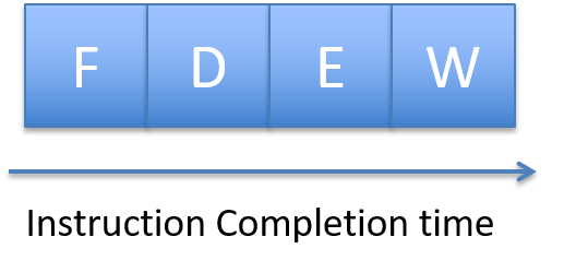
Because it takes one clock cycle to complete one stage of CPU instruction execution, a processor with a four-stage instruction execution sequence (Fetch, Decode, Execute, WriteBack; see Figure 8) completes at most one instruction every four clock cycles.
If, for example, the clock rate is 1 GHz, one instruction takes 4 nanoseconds to complete (each of the four stages taking 1 nanosecond). With a 2-GHz clock rate, one instruction takes only 2 nanoseconds to complete.
Although clock rate is a factor in a processor’s performance,
clock rate alone is not a meaningful measure of its
performance. Instead, the average number
of cycles per instruction (CPI) measured over a program’s
full execution is a better measure of a CPU’s performance.
Typically, a processor cannot maintain its maximum CPI for an
entire program’s execution. A submaximum CPI is the result of
many factors, including the execution of common program
constructs that change control flow such as loops, if-else branching, and
function calls. The average CPI for running a set of standard benchmark
programs is used to compare different architectures. CPI is a more accurate
measure of the CPU’s performance as it measures its speed executing
a program versus a measure of one aspect of an individual instruction’s
execution. See a computer architecture textbook1 for more details
about processor performance and designing processors to improve
their performance.
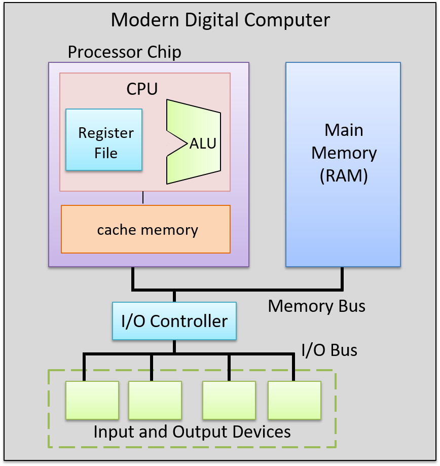
5.6.2. Putting It All Together: The CPU in a Full Computer
The data path (ALU, register file, and the buses that connect them) and the control path (instruction execution circuitry) make up the CPU. Together they implement the processing and control parts of the von Neumann architecture. Today’s processors are implemented as digital circuits etched into silicon chips. The processor chip also includes some fast on-chip cache memory (implemented with latch storage circuits), used to store copies of recently used program data and instructions close to the processor. See the Storage and Memory Hierarchy Chapter for more information about on-chip cache memory.
Figure 9 shows an example of a processor in the context of a complete modern computer, whose components together implement the von Neumann architecture.